Features of checking a transistor with a multimeter without soldering. How to test a transistor with a multimeter: testing various types of devices How to test live transistors in a circuit
Before considering ways to check the health of transistors, you need to know how to check the health of a p-n junction or how to properly test diodes. This is where we will start...
Semiconductor Diode Testing
When testing diodes using pointer ampere-volt-ohmmeters, the lower measurement limits should be used. When checking a working diode, the resistance in the forward direction will be several hundred Ohms, and in the reverse direction - an infinitely large resistance. If a diode malfunctions, a pointer (analog) ammeter will show a resistance in both directions close to 0 (if the diode breaks down) or an infinitely high resistance if the circuit is broken. The resistance of transitions in the forward and reverse directions is different for germanium and silicon diodes.
Diode check using digital multimeters is carried out in their testing mode. In this case, if the diode is working, the display shows the voltage at the p-n junction when measuring in the forward direction or a gap when measuring in the reverse direction. The magnitude of the forward voltage at the junction for silicon diodes is 0.5...0.8 V, for germanium diodes - 0.2...0.4 V. When checking a diode using digital multimeters in resistance measurement mode, when checking a working diode, it is usually there is a gap in both the forward and reverse directions due to the fact that the voltage at the multimeter terminals is not enough for the junction to open.
For the most common bipolar transistors, testing them is similar to testing diodes, since the structure of the pnp or npn transistor itself can be represented as two diodes (see the figure above), with the cathode or anode terminals connected together, representing the terminal of the transistor base. When testing a transistor, the forward voltage at the junction of a working transistor will be 0.45...0.9 V. Simply put, when checking the base-emitter, base-collector junctions with an ohmmeter, a working transistor in the forward direction has a small resistance and a large transition resistance in the reverse direction . Additionally, you should check the resistance (voltage drop) between the collector and emitter, which for a working transistor should be very large, except for the cases described below. However, there are some peculiarities when checking transistors. We will dwell on them in more detail.
One of the features is that some types of powerful transistors have a built-in damper diode, which is connected between the collector and emitter, as well as a resistor with a nominal value of about 50 Ohms between the base and emitter. This is typical primarily for horizontal scan output stage transistors. These additional elements disrupt the normal testing pattern. When checking such transistors, you should compare the parameters being tested with the same parameters of a known-good transistor of the same type. When checking transistors with a resistor in the base-emitter circuit with a digital multimeter, the voltage at the base-emitter junction will be close to or equal to 0 V.
 Other “unusual” transistors are composite transistors connected in a Darlington circuit. Outwardly, they look like ordinary ones, but in one case there are two transistors connected according to the circuit shown in Fig. 2. They are distinguished from ordinary ones by their high gain - more than 1000.
Testing of such transistors is no different, except that the forward voltage of the base-emitter junction is 1.2...1.4 V. It should be noted that some types of digital multimeters in test mode have a terminal voltage of less than 1.2 V , which is not enough to open the p-n junction, and in this case the device shows a gap.
Testing of unijunction and programmable unijunction transistors
A unijunction transistor (UJT) is distinguished by the presence of a section with negative resistance on its current-voltage characteristic. The presence of such a section indicates that such a semiconductor device can be used to generate oscillations (OPETs, tunnel diodes, etc.).
The unijunction transistor is used in oscillator and switching circuits. First, let's look at how a unijunction transistor differs from a programmable unijunction transistor. It is not difficult:
- What they have in common is a three-layer structure (like any transistor) with 2 p-n junctions;
- A unijunction transistor has terminals called base 1 (B1), base 2 (B2), and emitter. It enters the conducting state when the emitter voltage exceeds the critical switching voltage and remains in this state until the emitter current drops to a certain value called the turn-off current. All this is very similar to the operation of a thyristor;
- A programmable unijunction transistor has terminals called anode (A), cathode (K) and control electrode (GE). According to the principle of operation, it is closer to a thyristor. It switches when the voltage at the control electrode exceeds the voltage at the anode (by approximately 0.6 V - the forward voltage of the p-n junction). Thus, by changing the voltage at the anode using a divider, you can change the switching voltage of such a device, i.e. "program" it.
To check the serviceability of a unijunction and programmable unijunction transistor, you should measure the resistance between terminals B1 and B2 or A and K with an ohmmeter to check for breakdown. But the most accurate results can be obtained by assembling a circuit for testing unijunction and programmable unijunction transistors (see the diagram below - for OPT - figure on the left, for programmable OPT - figure on the right).

Checking digital transistors

Rice. 4 Simplified circuit of a digital transistor on the left, Test circuit on the right. The arrow means "+" of the measuring device
Other unusual transistors are digital (transistors with internal bias circuits). Figure 4 above shows a diagram of such a digital transistor. The values of resistors R1 and R2 are the same and can be either 10 kOhm, or 22 kOhm, or 47 kOhm, or have mixed values.
A digital transistor is no different in appearance from a regular one, but the results of its “diagnosis” can confuse even an experienced technician. For many they were “incomprehensible” and remain so. In some articles you can find the statement - “testing digital transistors is difficult... The best option is to replace it with a known-good transistor.” Undoubtedly, this is the most reliable method of verification. Let's try to figure out if this is really so. Let's figure out how to properly test a digital transistor and what conclusions to draw from the measurement results.
To begin with, let us turn to the internal structure of the transistor, shown in Fig. 4, where the base-emitter and base-collector junctions are depicted for clarity in the form of two back-to-back diodes. Resistors R1 and R2 can be of the same value, or they can be different and be either 10 kOhm, or 22 kOhm, or 47 kOhm, or have mixed values. Let the resistance of resistor R1 be 10 kOhm, and R2 - 22 kOhm. Let us take the resistance of an open silicon junction to be 100 Ohms. In particular, this value is shown by the Ts4315 dial avometer when measuring resistance at the x1 limit.
In the forward direction, the base-collector circuit of the transistor in question consists of a series-connected resistor R1 and the resistance of the base-collector junction itself (VD1 in Fig. 1). The junction resistance, since it is significantly less than the resistance of resistor R1, can be neglected, and this measurement will give a value approximately equal to the value of the resistance of resistor R1, which in our example is 10 kOhm. In the opposite direction, the junction remains closed and no current flows through this resistor. The avometer needle should show “infinity”.
The base-emitter circuit is a mixed connection of resistors R1, R2 and the resistance of the base-emitter junction itself (VD2 in Fig. 4 on the left). Resistor R2 is connected in parallel to this junction and practically does not change its resistance. Therefore, in the forward direction, when the junction is open, the ampere-volt-ohmmeter will again show a resistance value approximately equal to the resistance value of the base resistor R1. When the polarity of the tester is changed, the base-emitter junction remains closed, and current flows through the series-connected resistors R1 and R2. In this case, the tester will show the sum of these resistances. In our example it will be approximately 32 kOhm.
As you can see, in the forward direction, a digital transistor is tested in the same way as a conventional bipolar transistor, with the only difference being that the arrow of the device shows the resistance value of the base resistor. And from the difference in the measured resistances in the forward and reverse directions, you can determine the resistance value of resistor R2.
Now let's look at testing the emitter-collector circuit. This circuit consists of two back-to-back diodes, and with any polarity of the tester, its arrow should show “infinity”. However, this statement is only true for a conventional silicon transistor.
In the case under consideration, due to the fact that the base-emitter junction (VD2) turns out to be shunted by resistor R2, it becomes possible to open the base-collector junction with the corresponding polarity of the measuring device. The transistor resistance measured in this case has some scatter, but for a preliminary assessment you can focus on a value that is approximately 10 times less than the resistance of resistor R1. When changing the polarity of the tester, the resistance of the base-collector junction should be infinitely large.
In Fig. 4 on the right summarizes the above, which is convenient to use in everyday practice. For a direct conduction transistor, the arrow will indicate “-” on the measuring device.
As a measuring device, it is necessary to use pointer (analog) AVOmeters with a head deflection current of about 50 μA (20 kOhm/V).
It should be noted that the above is somewhat idealized, and in practice, there may be situations that require logical interpretation of the measurement results. Especially in cases where the digital transistor turns out to be defective.
How to test a MOSFET
There are several different ways to test MOSFETs. For example this:
- Check the resistance between gate - source (3-I) and gate - drain (3-C). It must be infinitely large.
- Connect the gate to the source. In this case, the source-drain (IS) junction must be wired as a diode (an exception for MOS transistors that have built-in breakdown protection - a zener diode with a certain opening voltage).
The most common and characteristic malfunction of MOSFETs is a short circuit between the gate-source and gate-drain.
Another way is to use two ohmmeters. The first is switched on to measure between source and drain, the second - between source and gate. The second ohmmeter should have a high input resistance - about 20 MOhm and a voltage at the terminals of at least 5 V. When the second ohmmeter is connected in direct polarity, the transistor will open (the first ohmmeter will show a resistance close to zero), and when the polarity changes to the opposite, the transistor will close. The disadvantage of this method is the voltage requirements at the terminals of the second ohmmeter. Naturally, digital multimeters are not suitable for these purposes. This limits the use of this verification method.
Another method is similar to the second. First, the gate and source terminals are briefly connected to each other in order to remove the charge present on the gate. Next, an ohmmeter is connected to the source-drain terminals. Take a 9 V battery and briefly connect it with the plus to the gate and the minus to the source. The transistor will open and remain open for some time after the battery is disconnected due to the conservation of charge. Most MOSFETs turn on at a gate-to-source voltage of about 2 V.
When testing MOSFETs, special care must be taken to avoid damaging the transistor with static electricity.
How to determine the structure and pin locations of transistors whose type is unknown
When determining the structure of a transistor, the type of which is unknown, you should, by searching through six options, determine the base terminal, and then measure the forward voltage at the transitions. The forward voltage at the base-emitter junction is always several millivolts higher than the forward voltage at the base-collector junction (when using a dial multimeter, the resistance of the base-emitter junction in the forward direction is slightly higher than the resistance of the base-collector junction). This is due to transistor manufacturing technology, and the rule applies to ordinary bipolar transistors, with the exception of some types of power transistors that have a built-in snubber diode. The polarity of the multimeter probe connected when measuring transitions in the forward direction to the base of the transistor will indicate the type of transistor: if it is “+” - a transistor of the n-p-n structure, if “-” - the p-n-p structure.
How to test a transistor?(Or how to ring a transistor) Unfortunately, this question arises for everyone sooner or later. The transistor can be damaged by overheating during soldering or improper operation. If a fault is suspected, there are two easy ways to check the transistor.
How to check a transistor with a multimeter (tester)
Checking the transistor with a multimeter (tester) (transistor continuity) is done as follows.
For a better understanding of the process, the figure shows a “diode analogue” of an NPN transistor. Those. The transistor seems to consist of two diodes. The tester is installed to test diodes and ring each pair of contacts in both directions. There are six options in total.
- Base - Emitter (BE)
- Base - Collector (BC): The connection must behave like a diode and
conduct current in only one direction. - Emitter - Collector (EC): connection must not conduct current in any direction.
When testing a PNP transistor, the “diode analogue” will look the same, but with inverted diodes. Accordingly, the direction of current flow will be reversed, but also only in one direction, and in the case of “Emitter - Collector” - in no direction.
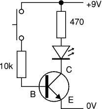
Assemble a circuit with a transistor as shown in the figure. In this circuit, the transistor acts as a “switch”. Such a circuit can be quickly assembled on a printed circuit board, for example. Pay attention to the 10Kohm resistor, which is included in the base of the transistor. This is very important, otherwise the transistor will “burn out” during the test.
If the transistor is working properly, then when you press the button the LED should light up and when released, it should go out.
This circuit is for testing NPN transistors. If you need to check the PNP transistor, in this circuit you need to swap the LED contacts and connect the power supply the other way around.
Thus, we can say that checking a transistor with a multimeter is simpler and more convenient. In addition, there are multimeters with a function for checking transistors. They show the base current, collector current and even the gain of the transistor.
And remember, no one dies as quickly and as silently as a transistor.
Semiconductor elements such as transistors are an integral part of almost all electronic circuits - from radio receivers to motherboards of highly complex computer centers. Checking this element for functionality is an operation that any person who is in one way or another involved in repairing electronic boards, be it a professional repairman or an amateur, must be able to perform.
To carry out this operation, you can use a special transistor tester, but if it is not at hand, or there are doubts about its reliability, you can use the most ordinary multimeter. Even those models that do not have a special socket for testing bipolar or field-effect transistors can be used for accurate testing. To do this, the multimeter is set to maximum resistance mode, or “continuity” mode, if there is one.
General verification algorithm
How to test a transistor with a multimeter? In general, the algorithm looks like this:

Further verification steps will depend on what type of element needs to be checked. Basically, semiconductor elements of two types are used in electronics - bipolar and field-field.
Bipolar
How to test a bipolar transistor with a multimeter? First of all, you need to find out which of the two subtypes - npn or pnp it belongs to. To do this, let’s remember what a bipolar transistor is.
 This is a semiconductor element in which the so-called npn or pnp junction is implemented. N-p-n is the transition “electron - hole - electron”, p-n-p, respectively, on the contrary, “hole - electron - hole”. Structurally, it consists of three parts - emitter, collector and base. In fact, a bipolar is two conjugated ordinary diodes, in which the base is the common connection point.
In the pnp circuit, the transistor differs from its npn counterpart in the direction of the arrow in the circle - the arrow of the emitter junction. In a p-n-p circuit it is directed towards the base, in an n-p-n circuit it is directed vice versa.
You need to know this difference to check the bipolar transistor. A Pnp circuit is opened by applying a negative voltage to the base, and an Npn one by applying a positive voltage. But before this, it is necessary to find out which of the contacts of the transistor being tested is the base, which is the emitter, and which is the collector.
Please note that using the method described below to determine which of the contacts is the base, and which are the emitter and collector, it is possible only for a working element. The very fact that the transistor has passed this test indicates that it is most likely working.
The instructions here could be as follows:
- the red (positive) probe is connected to the first terminal that comes across, for example the left one, the black (negative) probe alternately touches the central and right ones. Fix the value “1” on the central one, and 816 Ohms, for example, on the right;
- The red probe of the multimeter is short-circuited with the central contact, the black one - alternately with the side ones. The device displays “1” on the left and some value, say 807, on the right;
- when the red probe of the multimeter contacts the right terminal, and the black probe contacts the left and center, we get “1” in both cases. This means that the base is defined - this is the right contact of the transistor. And the transistor itself is PNP type.
In principle, this is enough to say that the transistor is working. Now, to check its structure and the specific location of the emitter and collector, we short-circuit the black (negative) probe of the multimeter with the base, and the red one in turn with the left and center contacts.

The contact that gives a lower resistance value will be a collector contact (in our case, 807 Ohms). The larger one - 816 Ohms - is the emitter one.
Testing an NPN type transistor occurs in the same way, only the positive contact is applied to the base.
This is a way to test p-n junctions between base and collector and base and emitter. The multimeter readings may vary depending on the type of transistor, but will always be within the range of 500-1200 Ohms. To complete the test, touch the emitter and collector probes. A working element will produce infinitely high resistance, regardless of its type, no matter how you change the polarity. If the value on the screen differs from “1”, one of the transitions is broken, the part is unusable.
Testing without soldering
If you are not sure that this particular transistor needs to be checked, you can measure its parameters on the board without desoldering. But at the same time, the multimeter should show values in the range of 500-1200 Ohms. If they are measured in units or even tens of Ohms, the circuit is shunted with low-resistance resistors. For an accurate check, the transistor will have to be unsoldered.
Field
A field-effect transistor, also known as a mosfet, differs from a bipolar transistor in that either only a positive charge or only a negative charge (“hole” or electron) can flow through it. Its contacts have a different meaning - gate, drain, source.
How to test a field-effect transistor with a multimeter? The testing technique is almost the same as in the previous case, but first, in order to avoid failure of the element, it is necessary to remove the charge of static electricity, since the field worker is very sensitive to static. Use an antistatic wrist strap, or simply touch your hand to a grounded metal part, such as a cabinet frame.
 Field devices always have a small conductivity between the drain and the source, which is detected on the multimeter screen as a resistance of the order of 400-700 Ohms. If you reverse the polarity, the resistance will change slightly, increasing or falling by 40-60 ohms. Before this, it is necessary to short-circuit the source and drain together in order to “zero” the capacitances of the junctions.
If, when tested with a multimeter, an infinitely large resistance is detected between the source and drain, the field effect transistor is faulty.
Conductivity will also be detected between source and gate or drain and gate, but only in one direction. A plus applied to the gate, and a minus to the source, will cause the transition to open and, accordingly, the value on the screen will be in the range of 400-700 Ohms. The reverse circuit - plus to the source, minus to the gate - for a working field operator will give “1”, that is. very high resistance.
Checking the drain-gate line is similar. If the source-gate or drain-gate line has conductivity in both directions, this means that the field-effect transistor is broken.
In conclusion, we need to say a few words about the composite type. A compound transistor is an element that combines two ordinary bipolar transistors (sometimes three or more). Testing with a multimeter is carried out similarly to the methodology for a simple “bipolar”.
In the process of repairing electronics, it is often necessary to check the functionality of the most common radio components - transistors.
There is a device specially designed for this - R/L/C/Transistor-meter, but it is not always available.
Therefore, it is useful to know how to test transistors, which will be discussed below.
A transistor consists of materials with special electrical properties - semiconductors. The latter are of two types:
- with n-conductivity (electronic);
- with p-conductivity (hole).
The simplest representative of semiconductor elements is a diode containing one p-n junction.
Transistors are more complex. There are two types of them: bipolar and field.
Bipolar
Also divided into two subgroups:
- with n-p-n junction;
- with p-n-p junction.
The components of a bipolar transistor are called emitter, collector and base. If we imagine this element in the form of two connected diodes, then the base will be their junction point.
To check a bipolar device, you need to recognize its type (n-p-n or p-n-p) and determine the purpose of the terminals (base, emitter and collector).
Field
 Also divided into two types:
- n-channel;
- p-channel.
In a field-effect transistor, the resistance of the current-carrying section is regulated by the electric field.
The components of the element are called source, drain and gate. The current moves from source to drain, regulation is carried out by the gate.
The design of modern field-effect transistors is supplemented by a diode installed between the source and drain.
Determining the base (gate) output
The easiest way to determine the purpose of the transistor's terminals (pinout) is to download the documentation for it. The search is carried out using markings on the body. This alphanumeric code is typed into the search bar and then “datasheet” is added.
If the documentation cannot be found, the base and other terminals of the bipolar transistor are recognized based on its features:
- pnp transistor: opens by applying negative to the base;
- npn transistor: opens by applying a positive voltage to the base.
They work like this:
- Set up the multimeter: the red probe is connected to the connector with the “V/” icon Ω " (positive potential), black - to the COM connector (negative potential), and the switch is set to the "continuity" mode or, if this is not the case, to the resistance measurement sector (icon " Ω ") to the top position (usually "2000 ohms").
- Define the base. The red probe is connected to the first terminal of the transistor, the black one - alternately to the others. Then red is connected to the second terminal, black again in turn to the 1st and 3rd. A sign that the red one is connected to the base is the same behavior of the device when the black probe comes into contact with other terminals. The device beeped both times or showed a certain final resistance on the display - the transistor is of the n-p-n type; The device was silent both times or displayed “1” on the display (no conductivity) - the transistor belongs to the pnp type.
- Collector and emitter recognition. To do this, connect a probe corresponding to the type of conductivity to the base: for an n-p-n transistor - red, for a p-n-p transistor: black.

Design of a field-effect transistor with a control p-n junction and an n-type channel a) with a gate on the substrate side; b) with diffusion seal
The second probe is alternately connected to the other terminals. When contacting the collector, the display shows a lower resistance value than contacting the emitter.
The terminals of the field effect transistor are usually marked:
- G: shutter;
- S: source;
- D: drain.
If there is no marking, the gate is detected using the same circuit as that of a bipolar transistor.
Field effect transistors are sensitive to static electricity. Because of this, their terminals are short-circuited with foil during storage, and before starting manipulations, wear an antistatic bracelet or at least touch a grounded metal object (instrument cabinet) to remove the static charge.
Checking the transistor with a multimeter
If the purpose of the terminals is known, the bipolar transistor is checked as follows:
- Prepare the multimeter as described above: the switch is moved to the “2K” position in the “ Ω "(resistance measurement) or in continuity mode, the black probe is plugged into the "COM" connector, the red one into the "V/ Ω ».
- Connect the probes to the emitter and collector, then swap them. Normally, in both cases the device does not produce a signal and displays “1”. Some terminal resistance indicates a breakdown.
- Connect a probe corresponding to its type of conductivity to the base: “hole” base (n-p-n type transistor) – red probe, “electronic” (p-n-p type transistor) – black.
- The second probe is connected in turn to the emitter and collector. Test results: the multimeter emits a signal, the display shows a resistance from 500 to 1200 Ohms - the transistor is working; there is no signal and the display shows one - an open circuit.
- Another probe is connected to the base, and the second one is short-circuited in turn with the emitter and collector. Results: no signal, “1” on the display – the transistor is working; the device beeps, the display shows a certain final resistance value - the transistor is broken.
The field device is checked as follows:
- Static electricity is removed from the element.
- Set up the multimeter according to the usual scheme: black probe - into the “COM” port; red - to port “V/ Ω "; switch - to position “2K” of sector “ Ω "(resistance measurement).
- Check the resistance between drain and source: normally the tester displays 400 - 700 Ohms.
- The source and drain are short-circuited in order to reset the junction capacitances, after which the polarity is changed and the measurements are repeated. If the transistor is working properly, the readings change up or down by about 10% (40 - 70 Ohms). An infinitely high resistance between the source and drain (the display shows “1”) indicates a malfunction of the device.
- Check for one-way continuity between source and gate, then between drain and gate. With one polarity of measurements, the multimeter will show a resistance of 400 - 700 Ohms, with the other - unity. Which probe is connected to the gate depends on the type of transistor (n-channel or p-channel). If the conductivity on the drain-gate or source-gate lines is two-way, that is, the device displays a certain final resistance value at any polarity, the transistor is broken.
- When checking an n-channel field switch, the black probe is connected to the drain, the red probe to the source. The channel resistance value is recorded.
- The red probe is connected to the gate, which will lead to a partial opening of the transition.
- Return the red probe to the source and measure the channel resistance. If the transistor is working properly, the resistance will decrease (due to partial opening).
- The black probe is connected to the gate, which will close the transition.
- Return the black probe to the drain and measure the resistance. If the transistor is working properly, it takes on the original value that was recorded.

Transistor test circuit
Check points 6 - 10 for a p-channel field-effect transistor are performed with the opposite polarity - swapping the red and black probes.
The voltage generated by the multimeter is not enough to open the power transistors. In this case, a 12 V power supply is used, connected through a resistor with a resistance of 1500 - 2000 Ohms.
Testing without soldering
A bipolar transistor can be checked without soldering if the circuit is not shunted with low-resistance resistors. Otherwise, instead of a resistance of 500 - 1200 ohms, the multimeter will show only a few tens or even units. Then it is required.
Field-effect transistors are almost always bypassed, so they have to be desoldered before testing.
Gain Determination
When a device fails, another one with a similar gain is selected to replace it. To determine this parameter, you need a multimeter with a transistor testing function. On the switch panel of such a device there is a sector marked “hFE”. It has two rows of ports of three each, which are designated as follows:
- n-p-n;
- p-n-p.

Field effect transistor testing circuit
This is a type of bipolar transistor that needs to be connected to a given row of ports. The purpose of each port is judged by its letter designation:
- B: base;
- C: manifold;
- E: emitter.
By connecting the transistor leads to the corresponding ports of the appropriate row, the user sees the gain value on the display.
Checking a Composite Transistor
A compound transistor includes two conventional bipolar transistors, and sometimes more. The standard method of checking with a multimeter is not applicable to it. It is necessary to assemble an electrical circuit powered from a constant 12 V power source. “Plus” is connected through a light bulb to the collector, “minus” - to the emitter. The base is connected through a resistor to a switch, which allows you to apply either “plus” or “minus” to it.
The resistor resistance is calculated using the formula:
R = U x h21E /I,
- U - input voltage, V;
- H21E - minimum gain of this transistor;
- I - load current, A.
Consider the following example:
- tested composite transistor: KT827A (h21E = 750);
- lamp power: 5 W.
The load current will be: I = 5 / 12 = 0.42 A.
Then the resistor resistance: R = 12 * 750 / 0.42 = 21600 Ohm, take R = 21 kOhm.
The verification is carried out in two stages:
- Using a switch, “plus” is supplied to the base. If it is working properly, the light will come on.
- The switch short-circuits the base to minus.
If it is working properly, the light will go out.
Even the simplest multimeter, which is not equipped with a function for determining the parameters of semiconductor devices, will help check the performance of the transistor. If you need to select an equivalent one instead of a burnt-out transistor, you will have to look for a tester model with the mentioned function.
Let's get down to theory, wait a while to run away. The VashTekhnik portal, along with abstruse maxims designed to be understood by professionals, will provide the five-finger technique. Did not hear? Simple as five fingers. First, we will discuss the types of transistors, then we will tell you what can be done using a multimeter. Let's look at standard hFE sockets (we'll explain what they are) and a technique for replacing a circuit through connecting several diodes. We'll tell you where to start. You will understand how to test a transistor with a multimeter, or... Let’s, perhaps, without the “or”. Let's get started, in order to firmly distinguish a MOS transistor from a pug, let's explain the theory.
Types, classification of transistors
We avoid exploring the wilds. Know a simple rule: in bipolar transistors, carriers of both signs participate in creating the output current, in field-effect transistors - one. Definition of smart guys. Now we work with our fingers:
- Field-effect transistors are the beginning. When the Beatles took the stage, semiconductors began to replace vacuum triodes. In short, a pnp transistor is two crystal layers rich in positive carriers (silicon, germanium, impurity conductivity). While teaching physics lessons, the teacher often talked about how V-valent arsenic doped the silicon lattice, forming a new material. Let us add that the positive p-regions are fenced off by a narrow negative one (n-negative). Like a lump in my throat. A narrow isthmus, called the base, refuses to allow electrons (in our case, more like holes) to flow in the desired direction. A small negative charge appears on the control electrode, the collector holes (the upper p-region on traditional electrical circuits) can no longer be contained, literally tearing towards the applied voltage. Since the base is thin, using the accumulated speed, the carriers fly over the isthmus and are carried further - reaching the emitter (lower p-region), here they are carried away by the potential difference created by the supply voltage. Typical school explanation. The relatively small voltage of the control electrode is able to regulate the speed of a strong flow of holes (positive carriers) entrained by the supply voltage field. This is what the technology is built on. Electrons move towards the holes; transistors are called bipolar.
- Field-effect transistors are equipped with a channel of any type of conductivity that separates the source and drain regions (see figure above). The control electrode is called a gate. Moreover, the main material of the substrate, the gate, is opposite to the channel, source and drain. Therefore, positive voltage (see figure) prohibits the flow of charges through the transistor. The plus will pull (to the p-region) available electrons. Field-effect transistors are used much more often in electronics. In the figure, the gate is electrically connected to the crystal, the structure is called a control p-n junction. It happens that the region is isolated from the crystal by a dielectric, which is often an oxide. Pure MOSFET transistor, in Russian - MOS.

Using a multimeter, bipolar transistors are checked in normal mode. If the tester supports such an option, often called hFE, a round connector is mounted on the front panel, divided by a vertical line into two parts, where 4 sockets are labeled as follows:
- B – base.
- C – collector.
- E – emitter.
There are two emitter sockets to take into account the layout of the housing pins. The base can be on the edge or in the middle. Made for convenience. It makes no difference which socket the emitter leg of the bipolar transistor is inserted into. A few words on how to use it.
Checking a bipolar transistor with a multimeter in normal mode
In order for the bipolar transistor test socket to start working (taking measurements), we switch the tester to hFE mode. Where did the letters come from? h - concerns the category of parameters describing a four-terminal network of any type. It’s not important to know what the concept means - just let’s be clear: there is a whole group of h-parameters, among which there is one important one for those involved in electronics. Called common emitter current gain. Denoted by h21 (or by the lowercase Greek letter beta).
Digital mnemonics are poorly perceived by the human eye, so it was decided (abroad, of course) that F would denote forward current amplification, while E says that the measurement was carried out in a common emitter circuit (which is used in physics textbooks to illustrate the principles of operation of bipolar transistors). There are many switching schemes, each has advantages, the parameters can be characterized through h21 (some others mentioned in reference books). It is considered that if the gain is normal, the radio element is 100% operational. Now readers know how a pnp transistor or npn transistor is tested.
h21 depends on some parameters specified in the multimeter instructions. Supply voltage 2.8 V, base current 10 mA. Next, the graphics of the technical documentation (data sheet) of the transistor are taken, the professional knows how to find the rest. When the hFE mode is turned on and the legs of the bipolar transistor are connected to the required sockets, the current gain value of the device appears on the display. Take the trouble to compare the reference data, making adjustments for the measurement mode (if necessary). It just sounds complicated, just do it a couple of times yourself and you will achieve results.
Checking transistors with a multimeter: abnormal mode
Let's say the serviceability of a field-effect transistor is in doubt. The well-known Russian issue in electronics is present. They start to think... hmm.
- The field-effect transistor is unlocked or locked by a certain voltage sign. Discussed above. If you remember, they said that when testing, there is a small constant voltage on the tester probes. We will use it in our tests. While the transistor is on the board, it is difficult to make measurements; once it is removed from its usual environment, non-standard techniques can be used. It turns out that if an unlocking voltage is applied to the electrode, due to some of the transistor’s own capacitance, the area will charge, retaining the acquired properties. It is allowed to ring the electrodes between the source and drain. A resistance of about 0.5 kOhm will indicate that the field-effect transistor is operational. If you short-circuit the base with other taps, the conductivity will disappear. The field-effect transistor is closed and operational.
- Bipolar transistors, field-effect transistors with a control p-n junction, are much easier to check. In the first case, an equivalent circuit of the element is used with two diodes connected towards each other (or vice versa with their backs). Let's apply the unlocking voltage (p - plus, n - minus), obtaining a nominal value of 500 - 700 Ohms on the resistance meter. You can also make calls using your hearing. It’s not for nothing that a diode is often drawn on the scale. The dialer is used to check functionality. The voltage is enough to open the p-n junction.

Preparing to test the transistor
At times you will grab the compound transistor with your hands. There are several keys inside the case. It is used to save space while simultaneously increasing the gain (tens, thousands of times, if we were talking about a cascade circuit). This is how a Darlington transistor works. A protective zener diode is sewn into the case, protecting the emitter-base junction from overvoltage. Testing goes one way:
- You need to find detailed technical characteristics of the transistor (component element). At the current scale, computerization will not be a problem. Even if the product is imported. The symbols on the diagrams are clear, the terms are not complicated. The hFE parameter has been described.
- Then the study is carried out and the analysis is performed. Breaking down a circuit into simpler components. If a zener diode is connected between the collector and emitter junctions, it is logical to start testing with it. At the initial moment, the transistor is locked, the multimeter current will flow, bypassing the protective cascade. In one direction the zener diode will give a resistance of 500-700 Ohms, in the other (if it does not break through) there will be a break. Let's similarly break the Darlington transistor into parts, if you have an idea (discussed above).
The dialing mode will show the numbers. They say the voltage drop is, according to some sources, the nominal resistance. Let's try to bring experiments to solve the problem. Call a known good resistor, known by its resistance value. If the ohm value appears on the screen, there is nothing to think about. Otherwise, you can estimate the current at the same time (dividing the display potential by the nominal value). You also need to know, it will come in handy during the testing process. Before starting work, it is recommended to thoroughly study the multimeter. Take the instructions out of the trash can and read them.
People are interested in the question of whether it is possible to check the transistor with a multimeter without desoldering it. Obviously, a lot is determined by the scheme. The tester simply applies voltages and evaluates the resulting currents. Based on the readings, the gain is calculated, serving as a pass/fail criterion. Try checking the field-effect transistor with the multimeter included in the processor! Abandon hope, everyone who enters here. It is not always possible to test a field-effect transistor with a multimeter.
Break a bipolar transistor into diodes
The figure presented among the text shows a circuit replacing a transistor with two diodes. Allows us to consider the amplifying element, presenting it as the sum of two independent simpler ones. Not having amplification, exhibiting nonlinear properties (divergence of direct/reverse connection).
The multimeter is powerless to open the powerful transistors of the power circuits. Therefore, special circuits are used to test devices. You cannot test a bipolar transistor directly with a multimeter.

Checking conditional diodes replacing the transistor
There are several methods. You can try measuring resistance using a standard Ω scale. The red probe must be applied to the p-region. Then the multimeter display will show a number less than infinity. In the opposite direction the result will be zero. The multimeter will show a break. Normal diode test results.
If you use a special mode, the screen shows the size of the resistance in the forward direction, a break (standardly one in the left corner of the LCD screen) in the other. Please note that the figure contains explanatory notes on where to place the probe to obtain an open p-n junction. In the opposite direction, the device shows a break.
